
TL;DR
ASML has signed an agreement with Tata Electronics to supply lithography equipment for India’s first commercial semiconductor fab in Dholera, Gujarat. The project is part of an $11 billion investment and aims to establish India’s presence in advanced chip manufacturing.
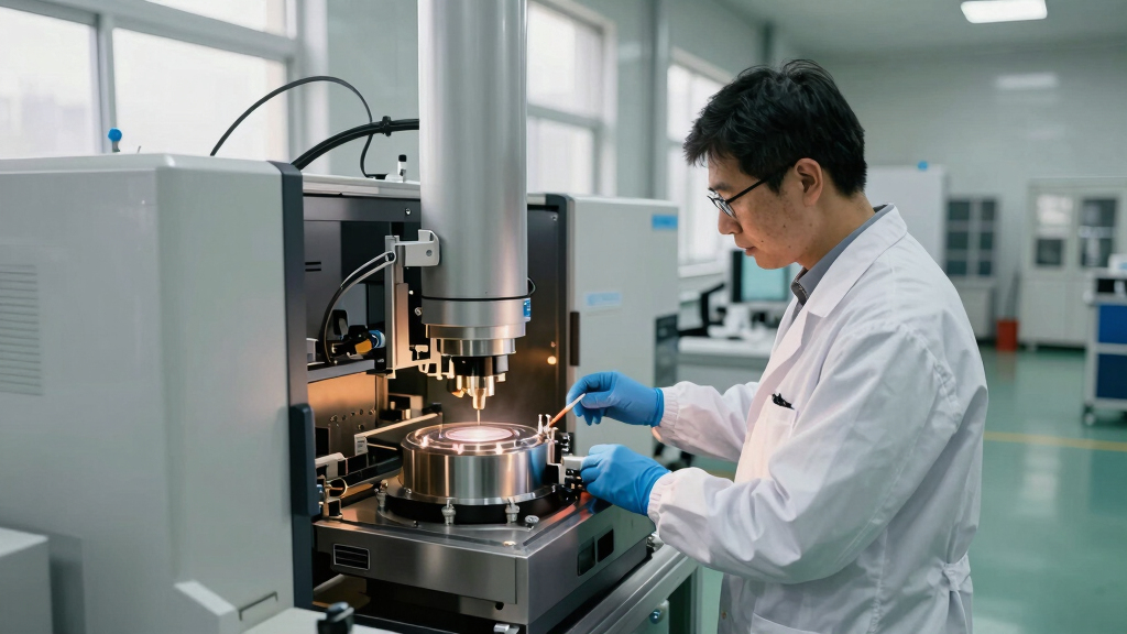
ASML has signed a memorandum of understanding with Tata Electronics to supply lithography equipment for India’s first commercial semiconductor fabrication plant in Dholera, Gujarat, marking a significant milestone in India’s chip manufacturing efforts.
The agreement was finalized during Indian Prime Minister Narendra Modi’s visit to the Netherlands, with Dutch Prime Minister Rob Jetten present. It covers the deployment of ASML’s advanced lithography tools, talent development initiatives, and supply chain support for the project.
The Dholera facility is a 300mm wafer fab with a total investment of approximately $11 billion. Civil construction at the site has reportedly reached about 50% completion. The project experienced a redesign late last year due to soil conditions found to be too soft and saline, but officials indicate this will not delay the overall timeline.
Trial production at the fab is still targeted for later this year, with the project seen as a major step toward establishing India as a player in advanced semiconductor manufacturing.
Why It Matters
This development is significant because it marks India’s entry into high-end chip manufacturing, which has traditionally been dominated by East Asian and American companies. The involvement of ASML, a leader in lithography technology, underscores the project’s technological ambitions and potential to boost India’s domestic semiconductor ecosystem.
It also signals increased international collaboration and investment in India’s semiconductor sector, which is viewed as strategically important for economic growth and technological sovereignty amid global supply chain shifts.
ASML lithography equipment
As an affiliate, we earn on qualifying purchases.
As an affiliate, we earn on qualifying purchases.
Background
India has been actively seeking to develop its semiconductor industry, with government initiatives aiming to attract investment and build manufacturing capabilities. The Dholera project is among the most prominent efforts, with civil construction progressing and plans to achieve trial production later this year.
ASML, based in the Netherlands, is the world’s leading supplier of lithography equipment critical for advanced chip fabrication. The recent deal was signed during Prime Minister Modi’s visit to the Netherlands, highlighting the diplomatic and strategic importance of the collaboration.
“Partnering with ASML is a major step forward in establishing India’s semiconductor manufacturing capabilities.”
— An official from Tata Electronics
“This collaboration exemplifies the strong technological ties between the Netherlands and India, and our shared commitment to advancing semiconductor innovation.”
— Dutch Prime Minister Rob Jetten
semiconductor fabrication tools
As an affiliate, we earn on qualifying purchases.
As an affiliate, we earn on qualifying purchases.
What Remains Unclear
It is not yet clear when the full deployment of ASML’s lithography equipment will be completed or when the fab will reach full production capacity. Details about the specific equipment models and timeline for operational readiness remain undisclosed.
300mm wafer fab equipment
As an affiliate, we earn on qualifying purchases.
As an affiliate, we earn on qualifying purchases.
What’s Next
Next steps include the installation and commissioning of ASML’s lithography tools at the Dholera site, with trial production expected later this year. Further updates are anticipated on the project’s progress and potential additional collaborations or investments.
advanced chip manufacturing machinery
As an affiliate, we earn on qualifying purchases.
As an affiliate, we earn on qualifying purchases.
Key Questions
What is the significance of ASML’s involvement in India’s chip industry?
ASML’s advanced lithography technology is essential for producing high-performance chips, and its involvement indicates a move toward cutting-edge semiconductor manufacturing in India.
When will the Dholera fab start producing chips?
Trial production is targeted for later this year, but full-scale commercial manufacturing will depend on equipment deployment and testing outcomes.
How does this project impact India’s technology ambitions?
This project marks a major step in establishing India as a player in advanced semiconductor manufacturing, reducing reliance on imports and strengthening its tech ecosystem.
What is the total investment in the Dholera project?
The project involves a total investment of approximately $11 billion.